Hermes Lite 2
- Details
- Hits: 3599
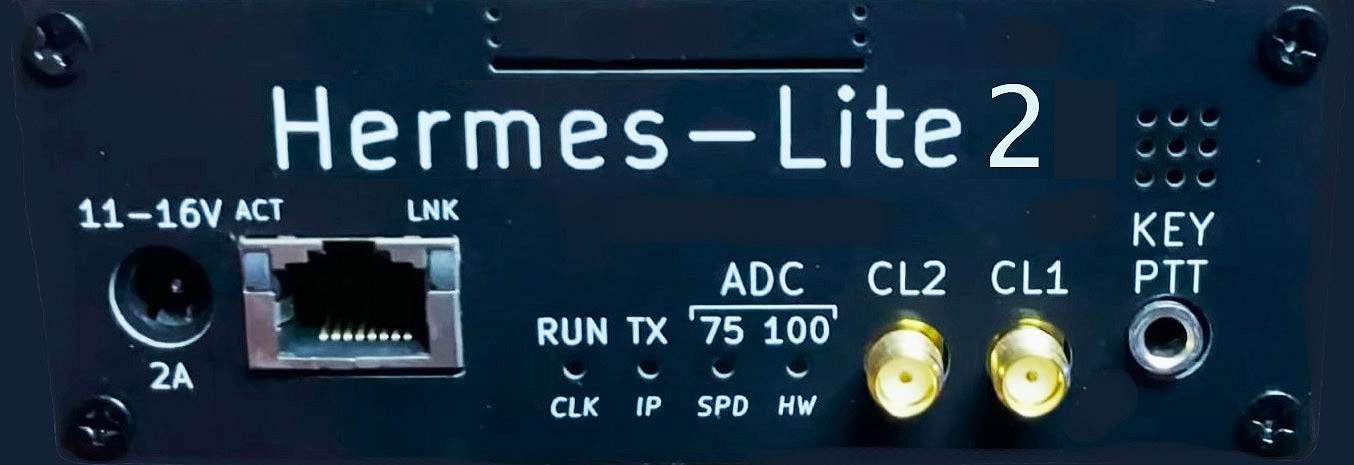 In December 2024 I decided to add the Hermes Lite 2 Software Defined Radio to my ham radio station. The Hermes Lite 2 is a low-cost, network-connected, direct down/up conversion software defined amateur radio HF transceiver based on the Analog Devices AD9866 broadband modem chip, the Altera Cyclone IV Field-Programmable Gate Array (FPGA) and the Hermes SDR project. It is entirely open source and open hardware, including the tools used for design and fabrication files. The RF output power is 5 Watts. The radio covers 130 kHz to 30 mHz. There is a wide choice of SDR software clients available for Windows, macOS, Linux, Raspberry Pi, or iPad, each with varying feature sets. Kits are available from Makerfabs. Among the software that works with the Hermes Lite 2 are Thetis, PowerSDR, SDR Console, SparkSDR and Quisk. SparkSDR allows you to load new gateware into the FPGA. Should updated gateware become available this is a nice feature. Some add-on accessories such as the Hermes Lite 2 + requires custom gateware. See more about the Hermes Lite 2+ below.
One big advantage of the Hermes Lite 2 is that, like the Anan radios from Apache Labs, it can run Pure Signal, also known as Adaptive Predistortion. Using a sampler at the output of your amplifier you can send your RF sample back to the radio where a program like Thetis can analyze it in real time and cause the Hermes Lite transmitter to provide equal and opposite adjustments to undesirable parts of the signal. This creates a very linear signal that causes almost no energy outside the passband of your desired signal.
My familiarity and fondness of the Anan 7000 SDR attracted me to the Hermes Lite 2 as a fun thing for experimentation as well as being a backup SDR. This board is a derivitave of the Hermes board found in the Anan 10 SDR originally available in 2012.
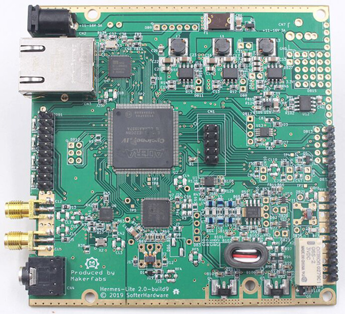 Above is a picture of the Hermes Lite 2 board from Makerfabs.
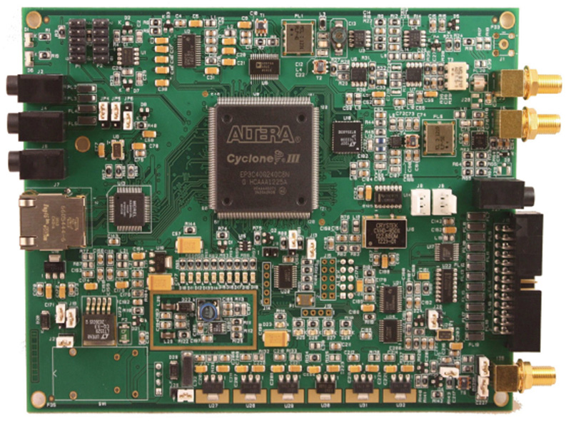 Above is a photo of the original Hermes board as found in the ANAN-10 SDR. The original Hermes board used the Altera Cyclone III Field-Programmable Gate Array (FPGA). The recent versions of the Hermes Lite 2 board use the Altera Cyclone IV FPGA which is a better device and offers greater performance. This is the same FPGA used in the Anan 7000 SDR.
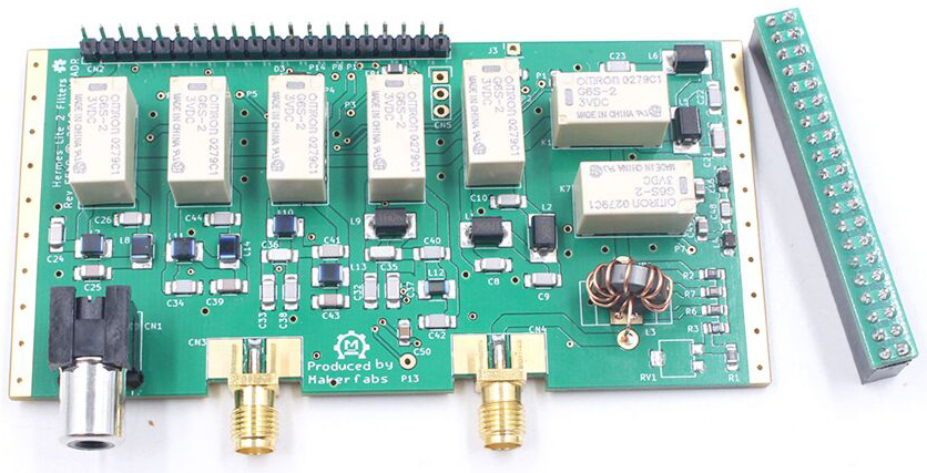
The Hermes Lite 2 needs an external filter board. It provides filters for the transmitter output to reduce its output harmonics and spurs and a receiver high-pass filter that can be used to remove strong broadcasts signals below 2 MHz. This board is also available on Makerfabs.
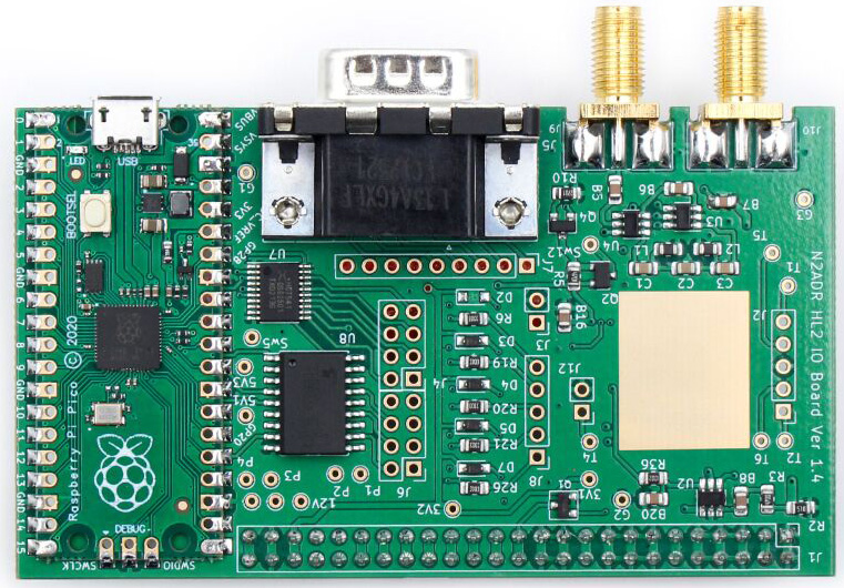
Next we have the I/O Board. This board connects to the Hermes Lite 2 and is mounted above the N2ADR filter board. It provides switches to control attached relays, antennas and power amplifiers. It also has a convenient jack to connect a sampler to run Adaptive Predistortion correction (Pure Signal).
The PC running the SDR software sends the transmit frequency to the I/O board. The Pico microcontroller on the board then uses the board's switches to control an amplifier, switch antenns or transverters. There are a variety of IO resources available and there will be different microcontroller software for each application. The IO board is meant to be a general purpose solution to control hardware attached to the HL2.
The user would have to load available programs into the Pico controller or write their own to take advantage of the board's features.
The DE-9 connector pins are available on the PCB pads on J7. The Pico GPIO pins are available on J4 and J6. The Outputs on J4 are TTL 5v levels. The Outputs on J6 are low-side switching MOSFET capable of handling loads of up to 50v and 500ma per channel. There is no protection here so diodes are needed across relay coils or other inductive loads. The Inputs are on J8. These five logic inputs are protected and work from +3.3 to +20v.
Depending on your application you would install header pins on J4, J6, J7 and J8. Then you would jumper the desired I/O pins on J4, J6 and J7 to the desired DE-9 pins on J7. The 9-pin jack on the edge of the board is often mistakenly called a DB-9 connector. It is really a DE-9. The E refers to the shell size (the body). The B shell size is the size of the common 25 pin DB-25 connectors.
I was initially confused that people were calling the Pico conroller a Raspberry Pi. Being familiar with Arduino and similar sized Arduino devices like the Nano I assumed the Pico was a variant of Arduino. This device creates a blur between Arduino and Raspberry Pi. The Pico has GPIO I/O Pins like the Raspberry Pi. This means the Pico can directly provide 5v control lines. The Pico can be programmed in C, C++, MicroPython or Circuit Python. MicroPython and Circuit Python permit programming on the device directly rather than compiling and transferring the code to the device. The Pico can be programmed using the Arduino IDE. The Pico does not have onboard Wifi.
The header of the I/O board has more pins than those soldered on the Hermes Lite 2 board so you have to solder the extra header pins to the HL2 board yourself.
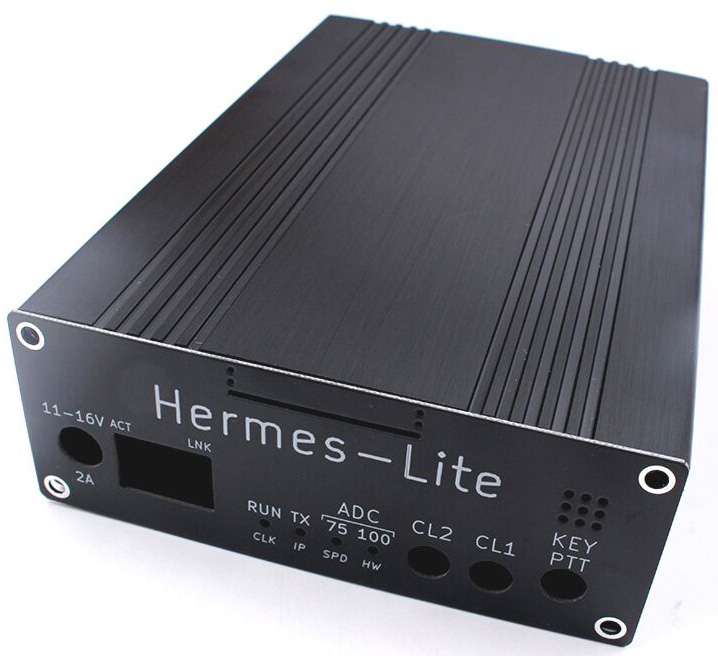
Finally we have the enclosure. This is an aluminum split shell with custom end plates. It is available from Makerfabs.
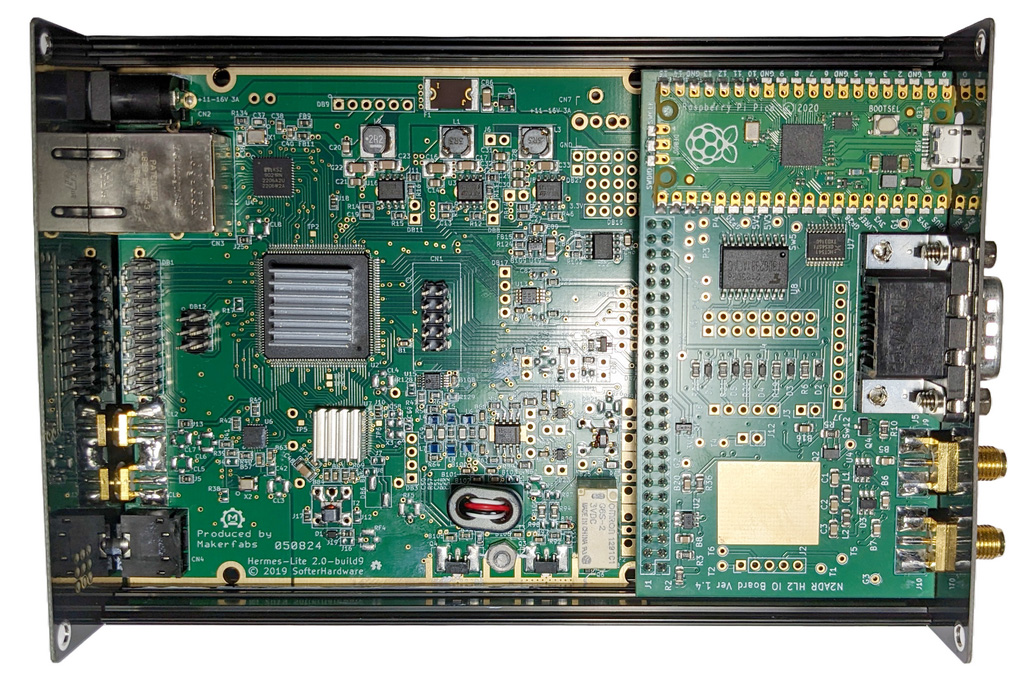
Here is a picture of my Hermes Lite 2 installed in the enclosure. On the left is the HL2 main board. To the right is the I/O Board. Under the I/O board is the filter board which is not visible in the photo. The J1 Header connects the three boards together. The I/O Board has a dual row female header that mates with the single row male pins on the HL2 board and the single row male pins on the N2ADR Filter board. The header on the I/O board bridges the header pins of the other two boards together.
There is another companion board using the AK4951 IC that claims to transform the Hermes LIte 2 into a Hermes Lite 2 Plus. This project is not affiliated with the official Hermes Lite 2 project and the use of the Hermes Lite 2 name was not authorized. The AK4951 basically creates a "sound card" inside the Hermes Lite 2.
The Hermes Lite 2 as it comes from Makerfabs has no analog audio in or out. Speaker and mic audio would be established through the ethernet cable using Virtual Audio Cable or cmASIO. That means your computer would need an audio device (sound card), speakers and a mic. You can use a built-in sound device on your laptop or desktop computer although a better option would be to obtain an external sound device that supports ASIO. The Hermes Lite 2 has no CW keyer or CW sidetone. You can connect a straight key or external keyer to the Key jack.
In the case of the AK4951 companion board, the audio is sent from the host software back to the "sound card" on the companion board. Tha audio latency on receive is not bypassed or improved. The AK4951 supports direct monitoring so you will hear your microphone audio or CW sidetone mixed in with no noticeable latency. The receive audio latency is still there but microphone/sidetone latency is not noticeable. If that is what you want you can achieve this by getting a better sound card with multiple inputs that supports direct monitoring. Plug your preferred keyer audio out into a sound card input, enable direct monitoring, and you have the same thing. The same is true for a microphone.
In order to use the Hermes Lite 2 Plus board and its features you have to load a custom version of the gateware into the FPGA on the main board. It does not use standard gateware. This makes the HL2 Plus effectively a separate branch outside of the main HL2 project. HL2 was designed as a network radio. The Plus variant breaks that philosophy by trying to make it a standalone radio. In either case, you still need a computer to run the HL2 or HL2 Plus. Why not connect the speaker and mic directly to the computer instead of connecting them to the radio, sending them from the radio to the computer over ethernet, and then sending them back to the radio from the computer over ethernet?
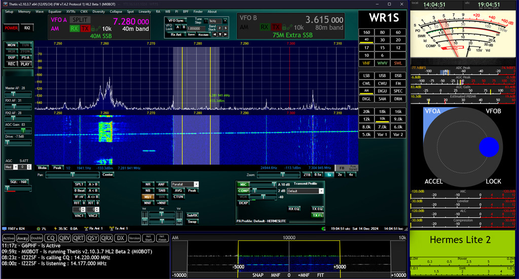
The Hermes Lite 2 would be worthless without software to control it and take advantage of its features. There is a version of the popuar Thetis program written for the Hermes Lite 2 that gives the same look and feel as the version used with the Anan series of radios. This is a screen shot of what my Hermes Lite 2 looks like on the computer screen. I don't have the Hermes Lite 2 Plus board so I can not connect a speaker, headphones or mic directly to my HL2. The only connections I have to the HL2 are power, antenna and etherent. All data, control and audio pass between the PC and the HL2 over the network cable.
There are plenty of assembly instructions and Youtube videos available online. Here are some links to get you started:
- Makerfabs
- Hermeslite.com
- N2ADR I/O Board
- Google Groups for Hermes Lite
- Hermes Lite Wiki
- Thetis Releases for Hermes Lite 2
Software that works with the Hermes Lite 2
| Software | Operating System |
| Thetis | Windows |
| PowerSDR | Windows |
| SDR Console | Windows |
| SparkSDR | Windows, Mac and Linux, Raspberry Pi |
| Quisk | Windows, Linux, Raspberry Pi |
| LinHPSDR | Linux |
| PiHPSDR | Raspberry Pi |
Makerfabs operates out of China. They have a good reputation as a reliable vendor who delivers a good product. The Hermes Lite 2 is marketed to technical type people who are expected to have some expertise. As such, you are expected to use community based support when you have problems. Justifyably, they are not quick to accept returns and you are expected to follow their directions to prove a defect before returning. All too often the "defect" is operator error. I have seen them quickly accept returns and provide replacements to resolve the few errors that happen at their end. All things considered there are many people who are happy with Maker Fabs and the Hermes Lite 2.
I opted to use the more expensive DHL shipping option just for peace of mind and the ability to track the shippment. My Hermes Lite 2 arrived ahead of their time estimate. It was well packed and double boxed. I used Paypal for payment.

